ece3400-2017
ECE 3400 Intelligent Physical Systems course web page and assignments
This project is maintained by CEI-lab
How to Design a PCB
ECE 3400, Fall 2017, Cornell University
By Leah Forrest and Kirstin Petersen, Nov. 11th 2017.
Here is the general process for PCB design:
-
Test your circuit on a breadboard. Be aware that continuous soldering and desoldering of components on a PCB can lead to ripped traces making the PCB useless - be sure that everything works up front!
-
When your circuit works, draw it up on a schematic. Be very sure that you pick the correct footprints for each component. (Insert video from Leah on libraries and schematic)
-
Then transfer the schematic to a PCB.
3.a. First, draw the outline of your PCB given the dimensions of your robot, mechanical constraints, etc. Mark up if there are any places where there are height restrictions for the components as well.
3.b. Add in mounting holes, and be sure they fit screws that are in the lab.
3.c. Second, add in your interface components - i.e. all connectors that needs to sit at the periphery of the board
3.d. Route the traces. Be sure to follow the constraints of the PCB manufacturer, i.e. consider minimum trace width and via size. Also, remember, if you are milling your own PCB, the vias are not necessarily through-plated, instead you must solder a piece of wires to connect the trace on the top and bottom layer. That also means that vias will not fit under a chip! (Insert video from Leah on trace routing)
3.e. What if I can’t connect my trace due to other traces? There are many ways to fix this. i) The expensive way is to add another routing layer (2 or 4 layers of copper for instance). ii) The simpler way is to add vias to which you can attach a separate wire. iii) If you are currently using surface mount components, you can swap one of them for a through-hole component, this typically allow you to route wires underneath the component.
3.f. Consider minimizing the size of your board. Does your components come with a different footprint? Can you place components on both sides of the board?
-
When you are finished, try printing it out on paper (be sure to print it un-scaled). That way you can easily test if everything fits on your robot/components. (Insert photo)
-
Finally, make a * .zip file and send it to kirstin_at_cornell_dot_edu. Use the following naming scheme: Date_TeamX_PCBrevX.zip. I.e. Team 1, sending their first PCB today would send 171018_Team1_PCBrev1.zip. Alternatively, if you are making the PCB on your own in the mill, generate Gerber files and follow your own usual procedures. (Insert Leah’s video on how to make Gerber files)
Here are several helpful hints to remember when designing your PCB:
- Add a power-on LED to visually indicate when your board is powered
- Always double- and triple check the footprints of your components, this is the number one cause of failures in PCB design.
- Print out the PCB top and bottom (unscaled) on paper first. That will allow you to test if it fits on your robot, if the components fit the footprints, if the connectors are in the right spot, etc.
- Never make right-angle traces. They do not conduct high frequencies well, they present a different impedance to your signals, and the sharp angle may cause differential strain when your robot vibrates that may break the trace.
- If your circuit consist of many parts, consider adding in jumpers that can be removed in case you only want to test parts of your circuit. This can help debugging.
- Add in extra measurement pads to ease debugging
- Choose components that are easy to solder. It takes some time to get really good at soldering small SMD components, so it you don’t need them, don’t bother using them. Through-hole resisters, and DIP-chips are handy - they also minimize the number of additional vias that you need to add to route traces on both sides of the PCB.
- Trace width can be chosen according to the current they carry. Smaller traces allow smaller PCBs. On the other hand, larger traces allow more flexibility if you have to hack the board later, and are less likely to peel off the surface from overheating with a soldering iron. 32mil width works well for standard traces.
- The PCBs that we will make in this class will not have silk-screens. However, you can still add text (like your team number/date) as copper traces on the board. We highly recommend doing this, so that we can tell all the boards apart. (Add photo of silk-screen)
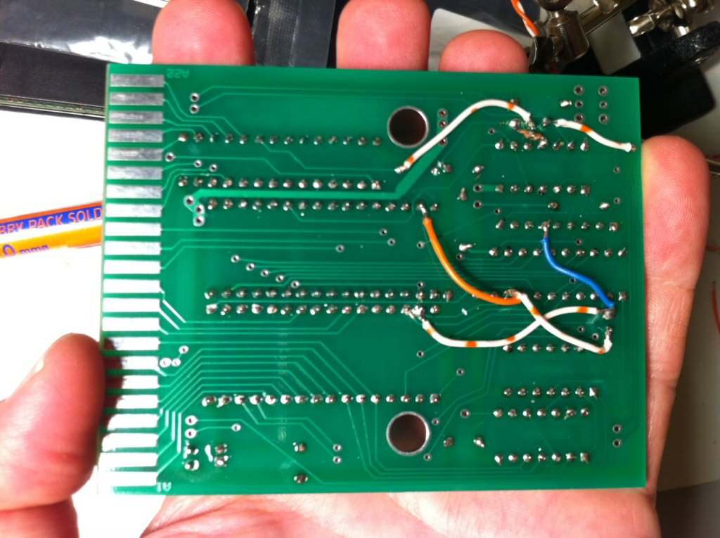
- Everyone makes mistakes on their first board, don’t worry if yours needs some hacks too. It is part of the learning process!
- Check out the class burn-list. This includes a brief description of all the things that didn’t work. In other words, if you learn something, please share it with us and we will add it to the burn-list to help future students!